1. Load a design.

  1. In the top-level directory, run the following command.

  2. Go to the physical design directory.

  3. In the directory, you will see the following files.

  4. Run EDI. You will see EDI graphyical user interface (GUI) window.

  5. Now, we will import the design. ("Import" is used for loading a design for the first time.)


2. Modify the layout area.

  1. In the main EDI window, click "Floorplan""Specify Floorplan ..."in the main menu.

  2. In the "Specify Floorplan" window, you will see the core utilization set to 0.7.

  3. Use the following settings for your design and click "OK". (Do not change other seetings).

  4. Now, you will see a modified floorplan as follows.

  5. Save your design. Click "File""Save Design". Choose "Encounter" instead of "OA". In the file name, type VRCA64_01_FL.enc and click "OK". Note that postfix "01_FL" denotes the current design step.
3. Power/ground routing

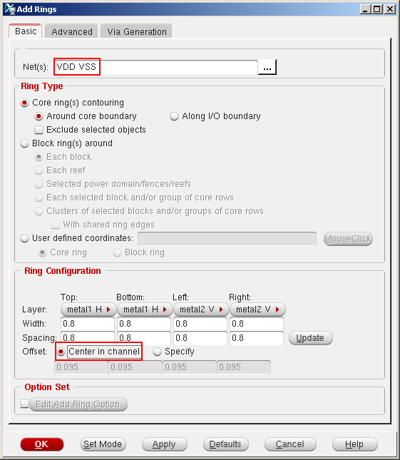
  1. Click "Power""Power Planning""Add Ring..." in the main menu. Use the following settings and click "OK".

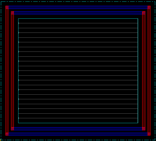
  2. You will see the following P/G rings.

  3. Now, you will route P/G lines for the standard cell rows. Click "Route""Special Route". Use the following settings and click "OK".

  4. You will see the following P/G network.

  5. Save your design into VRCA64_02_PG.enc.


4. Placement

  1. Click "Place""Place Standard Cell...". In the "Place" window, click "Mode" and change the "Specify Maximum Routing Layer" from 1 to 6. We will use only six metal layers. Click "OK" to apply the change and click "OK" again in the place window to run placement.

  2. Once the placement is done, click the following "Physical view" button to see the standard cells and wires.

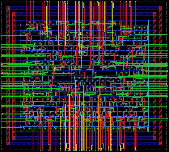
  3. The following shows my result.

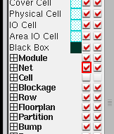
  4. In the "Layer Control" area in the GUI window, click the left check box button to turn off the visibility of the nets.

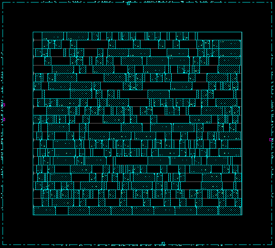
  5. Now, you will see your placement result as follows.

  6. Report timing. The slack in my run is -0.572ns. Since this is a ripple-carry adder, you will see the long carry chain in the timing report.

  7. Save your design into VRCA64_03_PL.enc.


5. Pre-CTS optimization

  1. Now, we will use text commands instead of GUI. Run the following command for preCTS optimization.

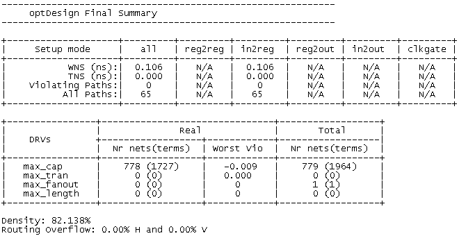
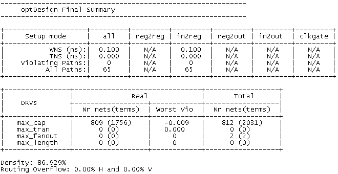
  2. The following shows my run. It satisfies the timing (WNS: 0.106ns).

  3. Report timing again. I get the same WNS value (0.106ns).


6. Clock tree synthesis (CTS)

  1. Click "Clock""Synthesize Clock Tree..." in the main menu. In the "Synthesize Clock Tree" window, choose "VRCA64_m.ctstch" for the "Clock Specification Files" and just click "OK". It will synthesize the clock tree.

  2. Report timing. I get 0.037ns WNS.


7. Post-CTS optimization

  1. Although we got positive WNS, let's run postCTS optimization.

  2. The following shows my optimization result.

  3. I got 0.100ns WNS.


8. Routing

  1. Click "Route""NanoRoute""Route..." in the main menu. Make sure the top layer is 6. Click "OK" to run nanoroute.

  2. You may see some "X" marks in the layout window after routing. They are design-rule violations. Let's ignore them.

  3. Report timing. I get 0.097ns slack.


9. Post-route optimization

  1. Run the following command.

  2. WNS in my run is -0.165ns.

  3. However, the utilization is already 99.2%. Further optimization might be useless.


10. Final timing analysis in PrimeTime

  1. Save your design.

  2. Click "Timing""Extract RC..." in the main menu. Check "Save SPEF to" and click "OK" to save the parasitic RC into the SPEF file.

  3. Save the final netlist.

  4. Close EDI.

  5. Source "synopsys.sh" in the top-level directory.

  6. Run PrimeTime.

  7. Run the following script.

  8. Report timing.

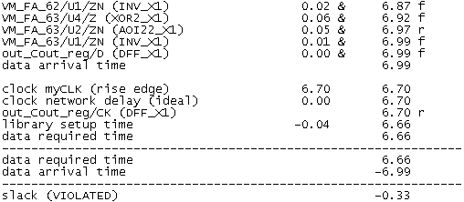
  9. In my run, the final slack is -0.33ns (violated).

  10. The following shows my log.